- Summary
- Table Of Content
- Methodology
Wafer Fabrication Market Size :
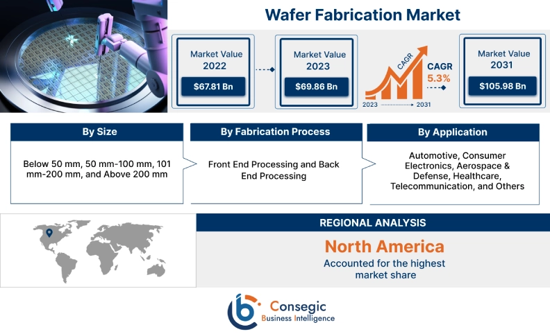
Wafer Fabrication Market size is estimated to reach over USD 108.37 Billion by 2032 from a value of USD 71.91 Billion in 2024 and is projected to grow by USD 74.41 Billion in 2025, growing at a CAGR of 5.3% from 2025 to 2032.
Wafer Fabrication Market Scope & Overview:
Wafer fabrication also known as semiconductor fabrication is the process of creating integrated circuits on semiconductor wafer. The wafers are thin, flat discs usually made from silicon and are key components of microelectronic devices. Moreover, wafer fabrication involves production of wafers in several sizes ranging from below 50 mm to above 200 mm. Additionally, wafers produced by a wafer fabrication process are used in various industries including automotive, consumer electronics, aerospace & defense, healthcare, telecommunication, and others.
Wafer Fabrication Market Insights :
Key Drivers :
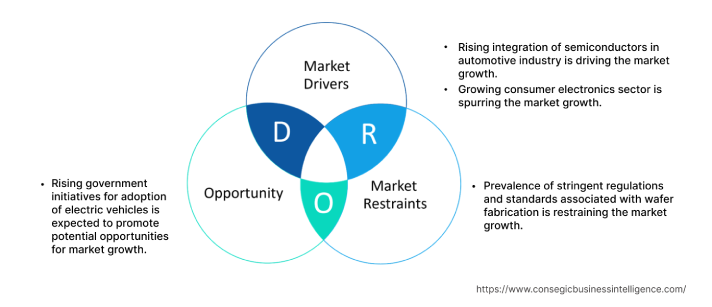
Rising integration of semiconductors in automotive industry is driving the market growth
Semiconductor wafers are primarily used in the automotive industry for processing and sensing critical data on the vehicle's computing systems to provide reliable, accurate, and timely control over the vehicle. Semiconductor wafers are used in various components of an automobile including switches, microprocessors, sensors, and other related automotive electronic components. Moreover, the utilization of semiconductor wafers in automobiles offers several benefits including enhanced connectivity, increased safety, advanced driving assistance, and others.
Factors including the advancements in autonomous driving systems, rising need for improved automobile sensor solutions, and increasing production of automobiles are among the primary determinants for driving the growth of the automotive industry.
According to the International Organization of Motor Vehicle Manufacturers, the total automotive production across the world reached 85.01 million in 2022, representing a growth of approximately 6% in comparison to 80.14 million in 2021.
Furthermore, according to the European Automobile Manufacturers Association, passenger car manufacturing in the Europe Union reached up to 10.9 million in 2022, demonstrating an incline of 8.3% as compared to 2021. Thus, an increase in automotive production is stimulating the market demand for wafer fabrication for manufacturing of semiconductor wafers for integration in the vehicle's computing systems, in turn driving the growth of the market.
Growing consumer electronics sector is spurring the market growth
Semiconductor wafers are used in the consumer electronics sector, specifically for production of integrated circuits utilized in smartphones, laptops, and other consumer devices. Semiconductors wafers are capable of controlling and managing the flow of electric current in electronic devices and equipment to ensure smooth operations. Moreover, the benefits of semiconductor wafers including compact size, high sensitivity to temperature and radiation, shock resistance, and others are increasing its utilization in the consumer electronics sector.
Factors including rising penetration of consumer devices, growing demand for miniaturized circuits in consumer electronic devices, and increasing integration of semiconductors in consumer electronic devices are key prospects driving the growth of the market.
For instance, according to the Association of German Banks, the electronics industry in Germany attained a significant growth in 2021. The production and nominal sales of electronics industry witnessed a growth of 10% in 2021 as compared to 2020.
Further, according to Japan Electronics and Information Technology, the total production by electronics industry in Japan reached USD 95.2 billion in 2021, witnessing a growth of 9.9% in comparison to 2020. Therefore, the growth of electronics sector is driving demand for wafer fabrication for production of semiconductor wafers for application in smartphones, laptops, television, and other related devices, in turn proliferating the market growth.
Key Restraints :
Prevalence of stringent regulations and standards associated with wafer fabrication is restraining the market growth
Semiconductor wafers are used in a wide range of industries including automotive, consumer electronics, healthcare, and others. However, wafer fabrication providers have to comply with various stringent standards associated with the production of semiconductor wafers, which is a primary factor restricting the market growth.
For instance, wafer fabrication providers have to comply with various standards such as ISO (International Organization for Standardization) standard - ISO 9001, ASTM (American Society for Testing and Materials), SEMI (Semiconductor Equipment and Materials International) standards, and others.
ISO 9001 standard specifies specific requirements for a quality management system. Wafer fabrication organizations must comply with the ISO standard for demonstrating the ability to consistently provide products and services that meet regulatory and customer requirements.
Additionally, SEMI (Semiconductor Equipment and Materials International) standards govern the material use, safety, manufacturing, and communication protocols that must be addressed across semiconductor and wafer fabrication facilities. Therefore, the prevalence of the aforementioned standards associated with wafer fabrication is constraining the growth of the market.
Future Opportunities :
Rising government initiatives for adoption of electric vehicles is expected to promote potential opportunities for market growth
Wafer fabrication plays a crucial role in the production of semiconductors used in electric vehicles for fostering the development of efficient power management systems, powerful batteries, and advanced driver assistance systems. Additionally, electric vehicles require the integration of more semiconductor content as compared to conventional vehicles for electrification and efficient vehicle operations.
Factors including progressions in electro-mobility, accessibility to a broad range of models, eco-friendliness, and prevalence of subsidies and tax rebates are driving the adoption of electric vehicles. For instance, purchase incentives and tax benefits for electric vehicles are available in 21 countries listed in the European Union including Austria, Netherlands, Belgium, Spain, Ireland, Poland, and other countries as of 2022.
Furthermore, governments worldwide are framing policies and initiative for reducing pollution and increasing the deployment of electric vehicles, which is anticipated to stimulate the adoption of EVs.
Therefore, rising government initiatives for adoption of electric vehicles are projected to increase the demand for wafer fabrication for production of semiconductors integrated in EVs, in turn facilitating opportunities for market growth during the forecast period.
Wafer Fabrication Market Report Insights :
| Report Attributes | Report Details |
| Study Timeline | 2019-2032 |
| Market Size in 2032 | USD 108.37 Billion |
| CAGR (2025-2032) | 5.3% |
| By Size | Below 50 mm, 50 mm-100 mm, 101 mm-200 mm, and Above 200 mm |
| By Fabrication Process | Front End Processing and Back End Processing |
| By Application | Automotive, Consumer Electronics, Aerospace & Defense, Healthcare, Telecommunication, and Others |
| By Region | North America, Europe, Asia-Pacific, Latin America, and Middle East & Africa |
| Key Players | Taiwan Semiconductor Manufacturing Company Limited, Tokyo Electron Limited, Intel Corporation, Lam Research Corporation, Motorola Solutions Inc., Applied Materials Inc., KLA Corporation, STMicroelectronics, SOITEC, Samsung |
Wafer Fabrication Market Segmental Analysis :
By Size :
Based on the size, the market is segmented into below 50 mm, 50 mm-100 mm, 101 mm-200 mm, and above 200 mm. The 101-200 mm segment accounted for the largest revenue share in the year 2024. Wafers with sizes ranging from 101-200 mm are primarily used in the production of multiple electronic devices, including integrated circuits (ICs), optoelectronic devices, and microelectromechanical systems (MEMS). Moreover, wafers with 101-200 mm size range are deployed in various industries including consumer electronics, automotive, and healthcare among others.
For instance, in April 2022, Wolfspeed Inc. launched its new wafer fabrication facility for development of 200 mm wafer in New York, United States. The 200 mm wafer fab aims at driving industry-wide conversion from silicon to silicon carbide-based semiconductors. The wafer fabrication facility provides high wafer quality and higher yield. Therefore, the rising innovations associated with wafer size ranging from 101–200 mm is a prime factor proliferating the growth of the segment.
The above 200 mm segment is anticipated to register the fastest CAGR growth during the forecast period. Silicon wafers with sizes ranging above 200 mm are large wafers that are primarily utilized in the fabrication of microelectronic devices, including transistors and integrated circuits (ICs) among others. Moreover, wafers with size above 200 mm are used in various industries including telecommunication, automotive, and other industrial applications.
For instance, in March 2022, SOITEC introduced its new wafer fabrication facility at its headquarters in Bernin, France. The wafer fabrication facility is primarily developed for manufacturing new silicon carbide wafers up to 300 mm in size, for utilization in electric vehicles and industrial sectors. Thus, the rising development of wafer fabrication facilities for production of wafers with size above 200 mm is a key factor anticipated to drive the market during the forecast period.
By Fabrication Process :
Based on the fabrication process, the market is segregated into front end processing and back end processing. The front end processing segment accounted for the largest revenue share in the year 2024. In the front end fabrication process, circuits are usually formed on the surface of the wafer. Dozens to hundreds of semiconductors with same circuit are formed in a lattice-like arrangement in the surface of a wafer. Further, the transistor layer is composed at the bottom of the wafer while the semiconductors are made by forming several layers of wiring circuit above the transistor layer.
For instance, Applied Materials Inc. is among the wafer fabrication companies that offers various single-wafer front-end fabrication processes in its product portfolio. Hence, the rising development of front end fabrication process for wafer fabrication is a prime factor fostering the growth of the segment.
Back end processing segment is expected to witness fastest CAGR growth during the forecast period. In back end fabrication process, wafers are cut into separate dice. The dice is further embedded in packages that offer all the electrical contacts for connecting the component to a circuit board.
For instance, STMicroelectronics is a wafer fabrication company that consists of seven back-end wafer fabrication and test facilities in 9 countries across Asia and Europe. Thus, the prevalence of significant number of wafer fabrication providers offering back end processes for wafer fabrication is among the primary factors anticipated to drive the market growth during the forecast period.
By Application :
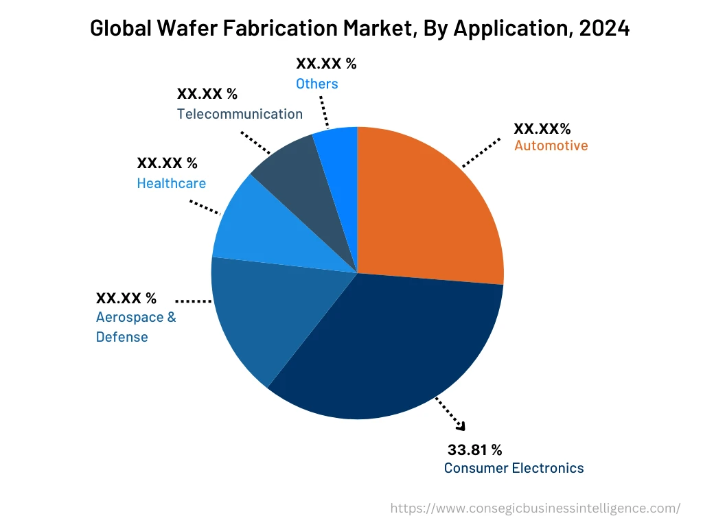
Based on the application, the market is segregated into automotive, consumer electronics, aerospace & defense, healthcare, telecommunication, and others. The consumer electronics segment accounted for the largest revenue share of 33.81% in the year 2024. Factors including rising penetration of consumer devices, increasing demand for miniaturized circuits in consumer electronic devices, and growing integration of semiconductors in consumer electronic devices are driving the growth of the consumer electronics segment.
For instance, according to GSM Association, the adoption of smartphones in Italy is anticipated to reach 81% by 2025, demonstrating a growth from 77% in 2021. Additionally, according to GSM Association, smartphone adoption in Germany is estimated to reach up to 84% by end of 2025, witnessing an incline from 80% in 2021. Therefore, the growth of consumer electronics sector is driving the demand for wafer fabrication for production of semiconductors for application in smartphones, laptops, tablets, and other related devices, in turn proliferating the growth of the market.
Automotive segment is expected to witness the fastest CAGR growth during the forecast period. The growth of automotive segment is attributed to several factors including growing investments in expansion of automotive manufacturing facilities, increasing production of automobiles, rising integration of advanced driver assistance system in modern automobiles, and advancements in autonomous driving systems.
For instance, according to the China Association of Automobile Manufacturers, the total production of passenger cars in China reached up to 14.8 million units in January-August 2022, witnessing a YoY growth of 14.7%. Wafer fabrication plays a crucial role in production of semiconductors used in various components of an automobile including switches, microprocessors, sensors, and other related automotive electronic components. Thus, rising automotive production is anticipated to drive the market growth during the forecast period.

By Region :
The regional segment includes North America, Europe, Asia Pacific, Middle East and Africa, and Latin America.

North America is estimated to reach over USD 35.12 Billion by 2032 from a value of USD 23.85 Billion in 2024 and is projected to grow by USD 24.64 Billion in 2025. The prevalence of significant number of wafer fabrication providers in North America including Intel Corporation, Lam Research Corporation, Applied Materials Inc., Motorola Solutions Inc., and others are contributing to market growth in the region. Moreover, the growth of automotive, aerospace & defense, healthcare, and other sectors is a vital factor driving the market demand for wafer fabrication in the region.
For instance, according to the International Organization of Motor Vehicle Manufacturers, the overall automotive production in North America reached 14,798,146 units in 2022, depicting a growth of 10% in comparison to 2021. Hence, the growing automotive industry is boosting the demand for wafer fabrication for manufacturing of semiconductors integrated in automobile electronic systems, in turn proliferating market growth in the North American region. Further, rising investments in electric vehicles and increasing demand for semiconductors from multiple industries are projected to drive the market growth in North America during the forecast period.
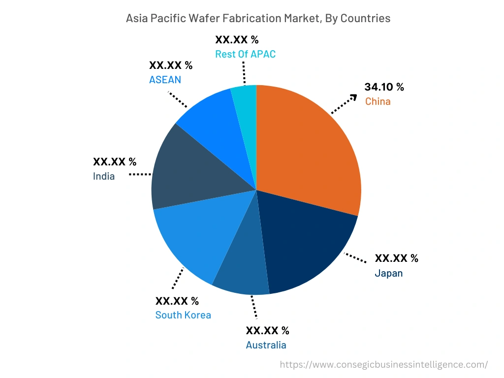
In Asia Pacific, the market is experiencing the fastest growth with a CAGR of 5.7% over the forecast period. In addition, in the region, the China accounted for the maximum revenue share of 34.10% in the same year.
The increasing pace of industrialization and development is providing lucrative growth prospects for the market in the region. Further, factors including the growth of multiple industries including consumer electronics, automotive, telecommunication, and others are driving the market growth for wafer fabrication in the Asia-Pacific region.
For instance, according to the India Brand Equity Foundation, the consumer electronics sector in India was valued at USD 9.84 billion in 2021, while it is estimated to grow at a significant rate to reach USD 21.18 billion by 2025. Therefore, the growing consumer electronics sector is anticipated to drive the market demand for wafer fabrication for production of semiconductors used in smartphones, laptops, tablets, and consumer appliances, thereby, boosting the market growth in the Asia-Pacific region during the forecast period.

Top Key Players & Market Share Insights:
The wafer fabrication market is highly competitive with major players providing wafer fabrication to the national and international markets. Key players are adopting several strategies in research and development (R&D), product innovation, and application launches to hold a strong position in wafer fabrication market. Key players in the wafer fabrication market include-
- Taiwan Semiconductor Manufacturing Company Limited
- Tokyo Electron Limited
- STMicroelectronics
- SOITEC
- Samsung
- Intel Corporation
- Lam Research Corporation
- Motorola Solutions Inc.
- Applied Materials Inc.
- KLA Corporation
Recent Industry Developments :
- In July 2023, July 2023, Applied Materials Inc. introduced its new wafer manufacturing platform Vistara that is designed to provide chipmakers with the intelligence, flexibility, and sustainability required to tackle growing chip making challenges.
Key Questions Answered in the Report
What is wafer fabrication? +
Wafer fabrication refers to a procedure composed of several recurrent sequential processes for manufacturing of complete photonic or electrical circuits on semiconductor wafers in semiconductor device fabrication process.
What specific segmentation details are covered in the wafer fabrication report, and how is the dominating segment impacting the market growth? +
For instance, by size segment has witnessed 101-200 mm as the dominating segment in the year 2024, owing to the increasing deployment of wafers with 101-200 mm size range in various industries including consumer electronics, automotive, and healthcare among others.
What specific segmentation details are covered in the wafer fabrication market report, and how is the fastest segment anticipated to impact the market growth? +
For instance, by application segment has witnessed automotive as the fastest-growing segment during the forecast period due to the rising adoption of semiconductor wafers in various automobile components including switches, microprocessors, sensors, and other related automotive electronic components.
Which region/country is anticipated to witness the highest CAGR during the forecast period, 2025-2032? +
Asia-Pacific is anticipated to register fastest CAGR growth during the forecast period due to rapid pace of industrialization and growth of multiple industries such as consumer electronics, automotive, telecommunication, and others.


